ES Electron, a customized solution for customers
BUSINESS
PCB
The best response at the lowest cost.


OSP
(Organic Solderability Preservative)It is a method of applying organic compounds to the copper surface of the PCB to prevent oxidation and maintain solderability.
As an eco-friendly smooth surface (lead-free and no hazardous substances), it is suitable for SMT (Surface Mount Technology).
HASL
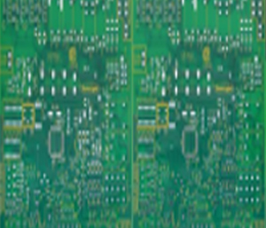
(Hot Air Solder Leveling)It is a method of applying lead and tin alloy to the PCB surface in a molten state and then flattening it with hot air to prevent oxidation and maintain electrical contact.
Advantages of good solderability and relatively long shelf life.
ENIG
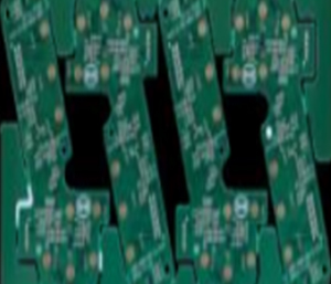
(Electroless Nickel Immersion Gold)It is a method of plating a thin gold over the nickel layer to protect the copper surface and provide good electrical contact.
It boasts excellent flatness and corrosion resistance, long shelf life, suitability for high density and high performance PCB, good solderability and reliability.
TIN
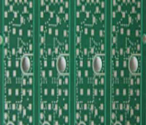
(Immersion Tin)It is a method of plating a thin layer of tin on the copper surface of the PCB to maintain solderability and prevent oxidation.
Having a flat surface, it is suitable for SMT, is eco-friendly (no lead), and involves low cost.
Via Hole Tenting
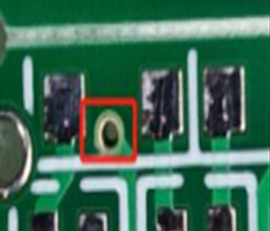
It covers the surface of the via hole with a solder mask, leaving the inside of the via unfilled.
It is good at protecting the via hole from coming into contact with outside air and moisture, streamlining the manufacturing process of PCB and reducing costs.
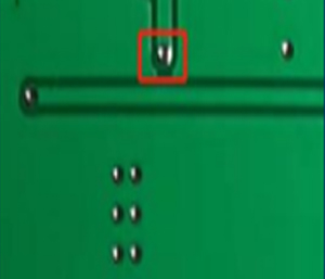
Via Hole with Window
It is a method of exposing the hole without applying a solder mask around the via hole. “Window” means that the hole is exposed.
The via is exposed for soldering. Holes enhance electrical connections or facilitate soldering.
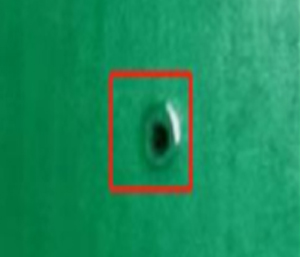
Plug Hole
A method of filling the inside of a via hole with a conductive or non-conductive material, which fills the hole and flattens it.
]It fills the interior to prevent the penetration of external materials and performs the final finish with a PCB surface flattening solder mask.
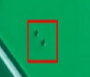
Resin Plug Hole
It is a method used for high-quality PCB design by filling via holes with resin, flattening the surface, and then finishing with metal plating.
It is mainly made of special materials such as resin, which completely fills the hole and performs additional flattening operations through subsequent processing. Smooth surface and high mechanical strength.
| Type | Key Features | Pros | Cons | Applications | |
|---|---|---|---|---|---|
| Surface Finish | OSP | Apply organic anti-rust agents | Low cost, eco-friendly | Less durable | Simple electronic devices |
| HASL | Apply lead/tin alloy | Low cost, long life | Uneven surface | General electronic devices | |
| ENIG | Nickel/gold-plated | High quality, long life | High cost | High-performance equipment | |
| TIN | Tin-plated | Good flatness, eco-friendly | Short retention period | Low-cost products | |
| Hole Processing | Tenting | It covers the via hole with a solder mask. | Low cost, simple process | Lacking strength, unsuitable for high-reliability requirement | Low-cost products, general circuit boards |
| With Window | It exposes the via hole. | Solderable, improved electrical reliability | Dust/moisture exposure hazard | Design with crucial electrical connections | |
| Plug Hole | It fills the inside of the via hole. | Protection and flattening, suitable for SMT | Increased costs, complex processes | High-density PCB, thermal management required products | |
| Resin Plug Hole | It fills the via hole with resin and treats it with metal plating. | High reliability, good electrical and thermal properties | High cost, complex process | High-performance/high-reliability PCB | |

